Schematics
From Rigol Homebrew Wiki
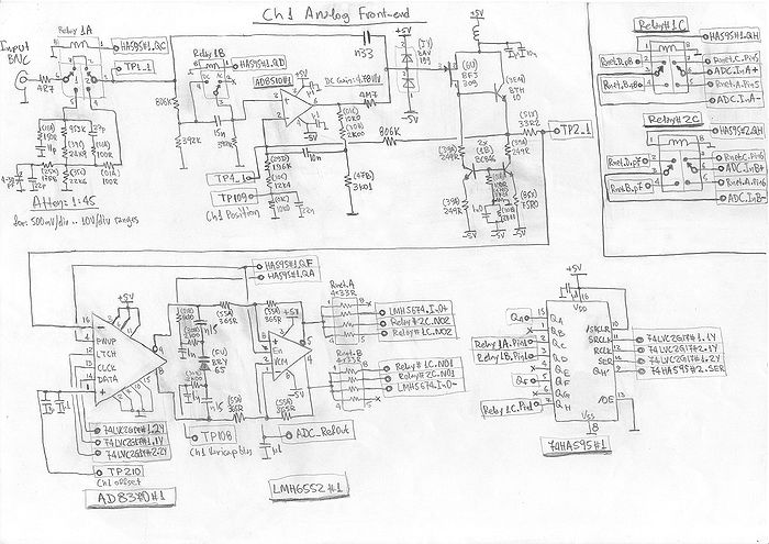
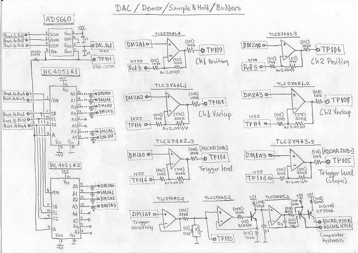
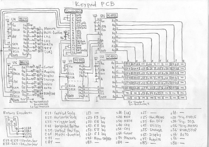
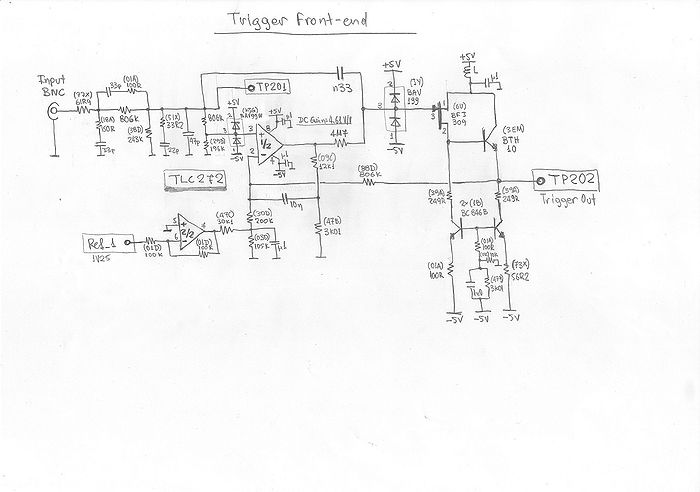
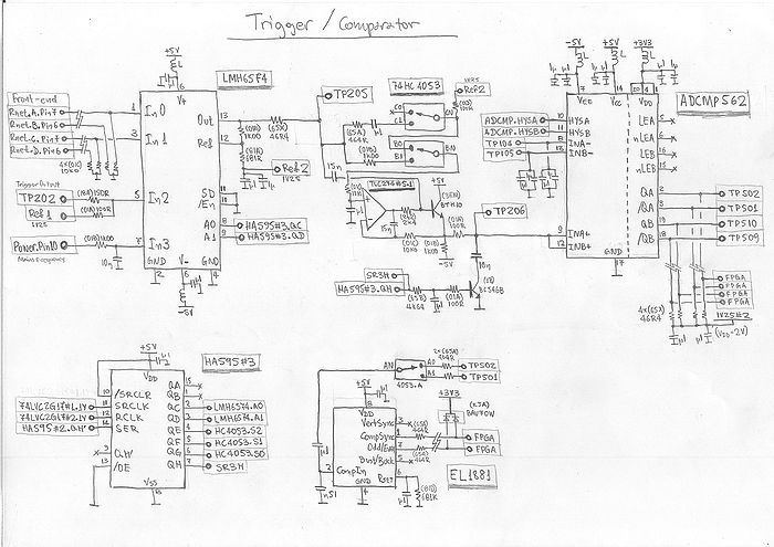
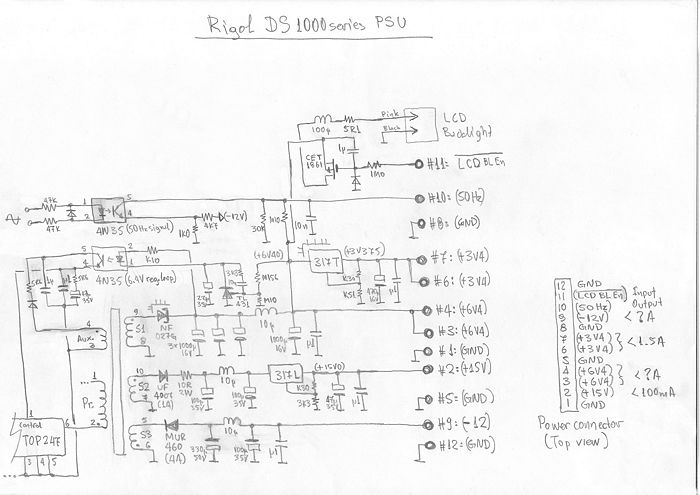
Here you will find some schematics from the Rigol DS1052/DS1102 Hardware Revision 58. The drawings comes from the user A Helene.
Contents
CH1 Analog Frontend
DAC, Demux, Sample & Hold, Buffers
Keypad PCB
Trigger input front-end
Trigger, Comparator
Power Supply Unit
Asynchronous Memory Bus
--------------------------------------------------------------------------------------
| - Asynchronous Memory bus:                                                         |
|------------------------------------------------------------------------------------|
|              Blackfin                   | CPLD  | FPGA  | LA     | FLASH  |ISP1362 |
|-----------------------------------------+-------+-------+--------+--------+--------|
|BF.162: ARDY    [I] Ready control (N/C)  |       |       |        |        |        |
|BF.154: /AOE    [O] Output Enable        |       |       | LH1.07 | FLR.28 |        |
|BF.153: /ARE    [O] Read Enable          | LT.85 | FP.E1 | LH1.10 |        |        |
|BF.152: /AWE    [O] Write Enable         | LT.86 | FP.E2 | LH1.09 |        |        |
|BF.161: /AMS0   [O] Bank Select 0        | LT.82 |       |        |        |        |
|BF.160: /AMS1   [O] Bank Select 1        | LT.81 |       |        |        |        |
|BF.159: /AMS2   [O] Bank Select 2        | LT.80 | FP.L8 |        |        |        |
|BF.158: /AMS3   [O] Bank Select 3        | LT.79 |       |        |        |        |
|BF.051: PF0/SS0 [?] ? (Pulled high)      |       |       |        |        |        |
|BF.050: PF1/SS1 [I] LA Ready (?)         |       |       | LH1.06 |        |        |
|BF.049: PF2/SS2 [I] USB INT1 output      |       |       |        |        | USB.30 |
|BF.034: PF10    [I] USB INT2 output      |       |       |        |        | USB.31 |
|BF.149: AADDR0  [O] USB A0: Command/Data |       |       |        |        | USB.61 |
|BF.148: AADDR1  [O] USB A1: Device/Host  |       |       |        |        | USB.62 |
| N/C            [-] USB /RD input        | LT.99 |       |        |        | USB.20 |
| N/C            [-] USB /CS input        | LT.100|       |        |        | USB.21 |
| N/C            [-] USB /WR input        | LT.01 |       |        |        | USB.22 |
| N/C            [-] LA ?                 | LT.83 |       | LH1.08 |        |        |
| N/C            [-] LA ?                 |       | FP.F6 | LH1.24 |        |        |
| N/C            [-] FLASH /WP            | LT.91 |       |        | FLR.14 |        |
| N/C            [-] FLASH /CE            | LT.98 |       |        | FLR.26 |        |
| N/C            [-] FLASH /WE            | LT.97 |       |        | FLR.11 |        |
| N/C            [-] FLASH ADDR19         | LT.96 |       |        | FLR.09 |        |
| N/C            [-] FLASH ADDR20         | LT.95 |       |        | FLR.10 |        |
| N/C            [-] FLASH ADDR21         | LT.94 |       |        | FLR.13 |        |
--------------------------------------------------------------------------------------
BF.x are the pins of BlackFin, [x] is the BlackFin pins direction, LT.x are the pins of the LaTtice CPLD, FP.x the pins of the Altera FPga, LH1.x those of the Logic Analyser Header 1 (the 40 pins one), FLR.x those of the Spansion FLash Ram and USB.x the pins of the Philips ISP1362 USB On-The-Go controller. All the components above share the same 16-bits data bus and the 21-bit Address bus; the BlackFin address bus is 19-bits wide, the address bus width of the CPLD, the FPGA and the Logic Analyser is 8-bits and the USB chip is controlled by the two lower address bus lines.
