Difference between revisions of "Schematics"
(→Keypad PCB) |
|||
| Line 13: | Line 13: | ||
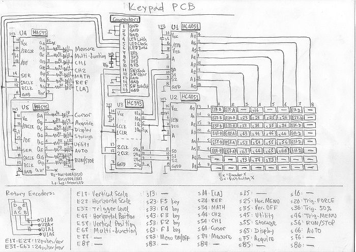
[[File:DS1052E HW58 PCB Schematics - Keypad PCB.jpg|700px]] | [[File:DS1052E HW58 PCB Schematics - Keypad PCB.jpg|700px]] | ||
| + | |||
| + | LED Shift Register connected to SPORT0 from Blackfin | ||
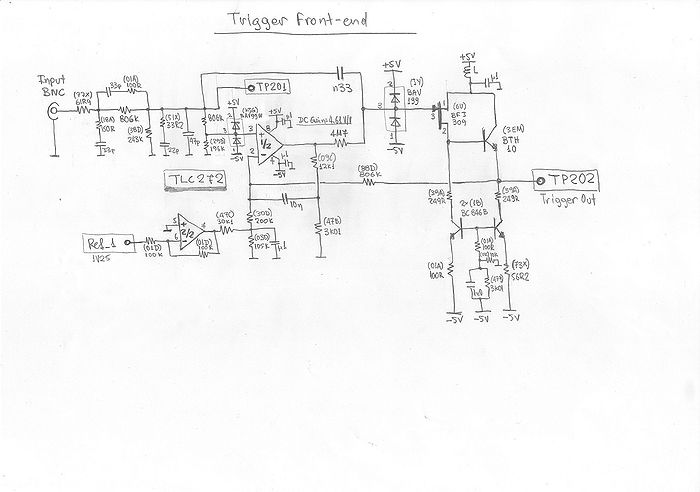
== Trigger input front-end == | == Trigger input front-end == | ||
Revision as of 13:34, 29 March 2013
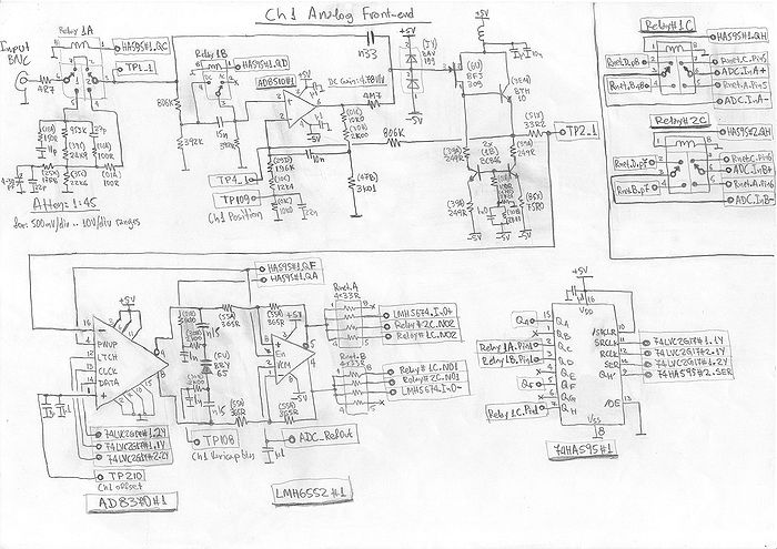
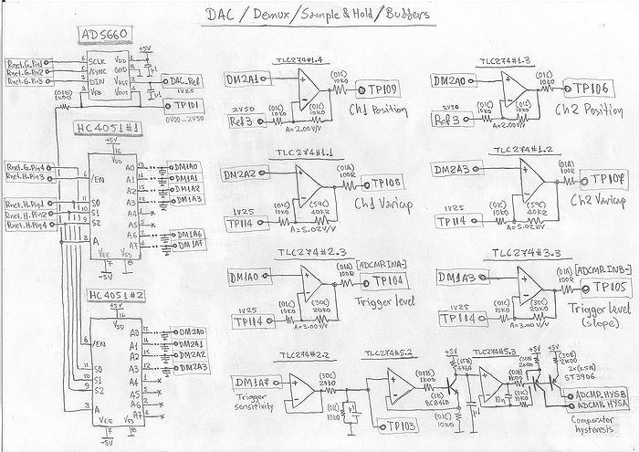
Here you will find some schematics from the Rigol DS1052/DS1102 Hardware Revision 58. The drawings comes from the user A Helene.
Contents
CH1 Analog Frontend
DAC, Demux, Sample & Hold, Buffers
Keypad PCB
LED Shift Register connected to SPORT0 from Blackfin
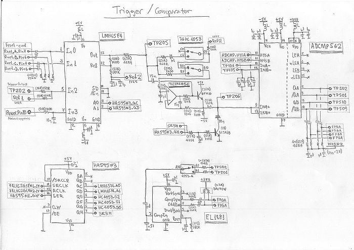
Trigger input front-end
Trigger, Comparator
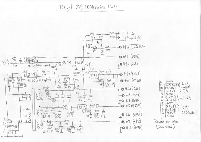
Power Supply Unit
Asynchronous Memory Bus
--------------------------------------------------------------------------------------
| - Asynchronous Memory bus:                                                         |
|------------------------------------------------------------------------------------|
|              Blackfin                   | CPLD  | FPGA  | LA     | FLASH  |ISP1362 |
|-----------------------------------------+-------+-------+--------+--------+--------|
|BF.162: ARDY    [I] Ready control (N/C)  |       |       |        |        |        |
|BF.154: /AOE    [O] Output Enable        |       |       | LH1.07 | FLR.28 |        |
|BF.153: /ARE    [O] Read Enable          | LT.85 | FP.E1 | LH1.10 |        |        |
|BF.152: /AWE    [O] Write Enable         | LT.86 | FP.E2 | LH1.09 |        |        |
|BF.161: /AMS0   [O] Bank Select 0        | LT.82 |       |        |        |        |
|BF.160: /AMS1   [O] Bank Select 1        | LT.81 |       |        |        |        |
|BF.159: /AMS2   [O] Bank Select 2        | LT.80 | FP.L8 |        |        |        |
|BF.158: /AMS3   [O] Bank Select 3        | LT.79 |       |        |        |        |
|BF.051: PF0/SS0 [?] ? (Pulled high)      |       |       |        |        |        |
|BF.050: PF1/SS1 [I] LA Ready (?)         |       |       | LH1.06 |        |        |
|BF.049: PF2/SS2 [I] USB INT1 output      |       |       |        |        | USB.30 |
|BF.034: PF10    [I] USB INT2 output      |       |       |        |        | USB.31 |
|BF.149: AADDR0  [O] USB A0: Command/Data |       |       |        |        | USB.61 |
|BF.148: AADDR1  [O] USB A1: Device/Host  |       |       |        |        | USB.62 |
| N/C            [-] USB /RD input        | LT.99 |       |        |        | USB.20 |
| N/C            [-] USB /CS input        | LT.100|       |        |        | USB.21 |
| N/C            [-] USB /WR input        | LT.01 |       |        |        | USB.22 |
| N/C            [-] LA ?                 | LT.83 |       | LH1.08 |        |        |
| N/C            [-] LA ?                 |       | FP.F6 | LH1.24 |        |        |
| N/C            [-] FLASH /WP            | LT.91 |       |        | FLR.14 |        |
| N/C            [-] FLASH /CE            | LT.98 |       |        | FLR.26 |        |
| N/C            [-] FLASH /WE            | LT.97 |       |        | FLR.11 |        |
| N/C            [-] FLASH ADDR19         | LT.96 |       |        | FLR.09 |        |
| N/C            [-] FLASH ADDR20         | LT.95 |       |        | FLR.10 |        |
| N/C            [-] FLASH ADDR21         | LT.94 |       |        | FLR.13 |        |
--------------------------------------------------------------------------------------
BF.x are the pins of BlackFin, [x] is the BlackFin pins direction, LT.x are the pins of the LaTtice CPLD, FP.x the pins of the Altera FPga, LH1.x those of the Logic Analyser Header 1 (the 40 pins one), FLR.x those of the Spansion FLash Ram and USB.x the pins of the Philips ISP1362 USB On-The-Go controller. All the components above share the same 16-bits data bus and the 21-bit Address bus; the BlackFin address bus is 19-bits wide, the address bus width of the CPLD, the FPGA and the Logic Analyser is 8-bits and the USB chip is controlled by the two lower address bus lines.
Programming connector
Info about the programming connector next to the usb port is required. Send any info to matt@yarrd.co.uk
- Matt
